
Replace various conductive materials with screen printing
Conductive ink that allows free setting of resistance value
Good news! For those who want to create electromagnetic wave shielding and implement electrostatic countermeasures inexpensively and effectively.
Thanks to adjustment technology of resistance value, effective electromagnetic wave shielding and electrostatic countermeasures are possible by screen printing. In addition, this adjustment technology expands the application possibilities such as quality improvement of sensor device and cost reduction of electronic circuits.
1. Conductive ink that enables you to set electrical resistance value freely
1.1 Achieve both screen ink function and flexible electrical resistance value
Our conductive ink can be set in a wide range of electrical resistance value from 1.0 x 10⁻¹ (Ω) to 1.0 x 10¹⁰ (Ω) or higher, from conductive to non-conductive. Owing to this ink, you can produce electromagnetic wave shielding and conduct electrostatic countermeasures, etc. with inexpensive and highly flexible screen printing.
In addition, by applying this conductive function to other inks, it is possible to improve sensor quality and reduce the cost for electronic circuits.

| Application |
Surface resistance value |
Main effects |
|---|---|---|
| Electromagnetic wave shield |
1.0×10⁻¹ to 1.0×10⁴ |
|
| Electrostatic countermeasures | 1.0×10⁴ to 1.0×10¹⁰ |
|
| Sensor quality improvement aid | Resistance value suitable for the application |
|
| Assist cost reduction of electronic circuits | Resistance value suitable for the application |
|
1.2 Basic performance of conductive ink
Standard conductive inks are as follows. Resistance values other than the following inks can also be set by adjusting ink and printing conditions. For example, the surface resistivity can be made lower than that of single-layer printing by using multi-layer printing.
| Ink name |
Ink layer thickness |
Surface resistance value | Applicable substrates |
|---|---|---|---|
| MRX-HF Conductive Ink Brown | 14µm | ≤ 1Ω | PET, PC, etc |
| MRX-HF Conductive Ink Gray | 14µm | ≤ 200Ω | Same as above |
| MRX-HF Conductive Ink Black | 10μm |
≤ 10,000Ω |
Same as above |
| GLS-HF Conductive Ink Black | 8µm | ≤ 2,000Ω | Glass, polyamide |
1.3 Common excellent features of conductive ink
Conventionally, electromagnetic wave shields and electrostatic countermeasures have been dealt with by methods such as using metal foil and conductive materials. However, printing conductive ink is a less expensive and more flexible method than the conventional method.
| Excellent features | Details |
|---|---|
| High moisture resistance, lightweight and thin |
|
| Inexpensive and flexible screen printing |
|
| Achieve both decoration and other functions |
|
2. Electromagnetic wave shielding ink
2.1 What is electromagnetic wave shielding ink ?
Electromagnetic wave shielding ink blocks electromagnetic wave from intruding or leaking into the printed ink layer. Thanks to this ink, it is possible to apply an electromagnetic wave shielding function by inexpensive screen printing.
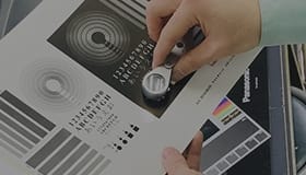
The following is an example of the printed material using electromagnetic wave shielding ink that blocks shields electromagnetic waves (in this case, radiated electric field) radiated from the computer screen. You can see the value of radiated electric field has been dropped from normal value of 128 (V/m) in the left photo to unmeasurable of 0 (V/m) in the right photo.

2.2 Printing example of electromagnetic wave shielding ink
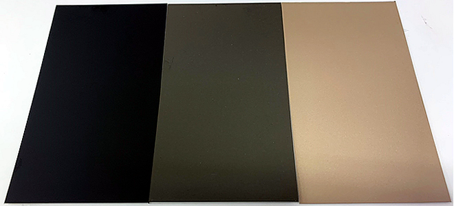
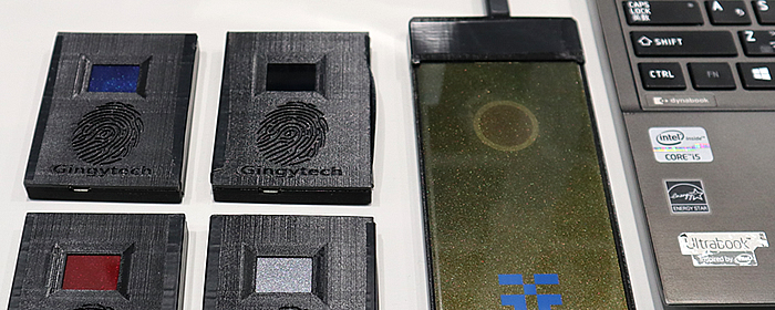
This is a printing example of black, gray and brawn of MRX-HF Conductive ink (substrate: PC) Achieving both an electromagnetic wave shielding function and decoration, it is possible to apply it to process reduction.
3. Anti-static measure ink
3.1 What is anti-static measure ink ?
Anti-static measure ink can add functions such as prevention of static charge, Electro-Static Discharge countermeasures by inexpensive screen printing.
For anti-static measure, it is necessary to appropriately adjust the electrical resistance value of the area where ink is printed according to the preconditions (usage environment, cause of electrostatic, etc.) and the problem to be solved (electrification, electric discharge, etc.). Therefore, anti-static measure ink, which allows you to freely set the resistance value and printed area, is one of the most ideal solution for them.
3.2 Electrical properties and surface resistivity used for anti-static measures
The following table shows the classification of electrical properties used for anti-static measures and advantages(Ο) and disadvantages(×) of each countermeasure. (Refer to: IEC 61340-5-1,5-2 Standard)
| Classification of electrical properties and Surface resistance value used ρs(Ω) | Characteristics and application to anti-static measures |
|---|---|
| Electrostatic conductivity 1.0×10² ≤ ρs < 1.0×10⁵ |
It is hard to be electrified but electrical charge moves faster ○ It unlikely becomes a source of electrostatic as it hardly electrifies. × There is a risk of electric discharge when a charged object comes into contact with it. |
| Electrostatic diffusivity 1.0×10⁵ ≤ ρs < 1.0×10¹¹ |
It is hard to be charged and electrical charge diffuses slowly (the area used for antistatic). ○ It is not easily charged by nature and even if it is electrified, it discharges relatively slowly. ○ Intense discharge does not occur even if a discharged substance comes to contact with it. × It is necessary to adjust resistance value according to the solution (charging conditions, desired charge decay, etc.) |
| Insulation 1.0×10¹¹ ≤ ρs |
It is easily charged and the charge is easily stored but the speed of transfer and diffusion is small. ○ Discharge does not occur as it does not energize even if a charged substance comes to contact with it. ○ It is a solution to reduce the risk of discharge under limited conditions. × It causes static electricity as it is easily charged by friction. |
3.3 Printing example of anti-static measure ink
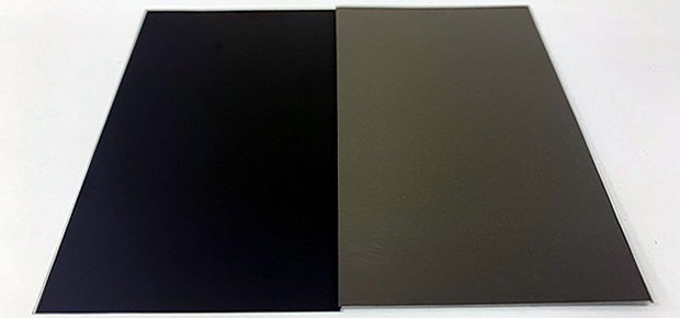
The photo below shows the printed material of GLS-HF Conductive ink Black and Gray (substrate: glass) Static charge can be prevented by setting the optimum resistance value in the electrostatic diffusivity region, which can solve problems such as discharge and dust adhesion, etc.
4. Application to quality improvement of sensor equipment
4.1 What is application to quality improvement of sensor equipment ?
The application to quality improvement of sensor equipment means that quality improvement can be realized by using conductive functions to solve deterioration of sensor sensitivity due to dust adhesion and sensor malfunction due to incident of electromagnetic waves. As these methods can be used with decoration process, compared with other methods, they can be implemented more easily than other methods.
| Application to sensor equipment | Beneficial effects |
|---|---|
| Anti-static measure |
|
| Electromagnetic wave shield |
|
4.2 Application example to quality improvement of sensor equipment
Applying anti-static measures to sensor ink for sensor light receiving port and ink for decorating housing, which prevents dust adhesion due to static electricity to the light receiving port and contributes to sensor sensitivity improvement.
5. Application to cost reduction of electronic circuits (Please contact us for details)
5.1 What is the application to cost reduction of electronic circuits ?
The application to cost reduction of electronic circuits means that replaces the elements and necessary functions used in electronic circuits by printing inexpensive and highly flexible conductive ink. This alternative method has a good compatibility with flexible circuits because its material is screen ink.
Note: As there is a case where printing is impossible depending on the content of alternation or problem to be solved, please feel free to get in touch with us for the specific issues and whether or not they can be solved by printing.
| How to apply to electronic circuit boards | Features |
|---|---|
| Replacement of resistor |
(Please feel free to get in touch with us for feasible resistance values, printing performance values, etc.)
|
| Replacement of other electron elements |
|
| Countermeasures against electromagnetic waves and static electricity |
|
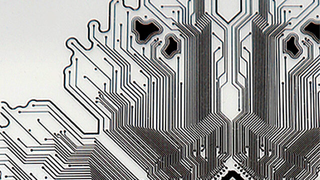
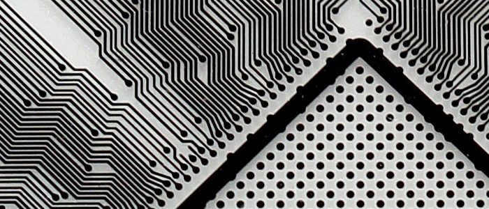
5.2 Substitution by printing of electronic circuit elements (the photo is just an image.)
The following is an image photo of electronic circuit substituted by screen printing elements. As for applying both conductivity and fine lines, limit values will vary depending on the conditions. If you are considering alternative electronic circuit elements (resistive elements, etc.) by printing, please feel free to contact us to discuss the possibility of solving your issue.
- Related technology information
- Related event information
- Related inks