
Past events
Exhibition Report of 29th FINETECH JAPAN
Event outline
The 29th LCD/OLED/Sensor Technology Expo (Finetech Japan) is a technology exhibition where everything from electronic displays (LCD, OLED, quantum dots, micro LEDs) to manufacturing equipment and material technologies are exhibited together.
We, at this technology exhibition, exhibited latest ink and printing technology such as Ink for Electromagnetic Wave Shield, Black Matrix, Sensor (IR Transmittable ink) and High Definition Ink (high-quality and high-definition screen ink), etc. .
- Period
- December 4 – December 6, 2019
- Venue
- Makuhari Messe, Japan
- Official HP
- https://www.ftj.jp/en-gb.html
List of Exhibits
- 1. Ink for electromagnetic wave shield that contributes to cost reduction, lighter weight and thinner shape
- 2. Introduction of Black matrix ink that contributes to significant cost reduction
- 3. Introduction of Ink for sensor (IR transmittable ink) that realizes seamless design
- 4. Introducing a new design with movement by concealing printing
- 5. Realize high-grade image by highly accurate printing. Introducing High Definition Ink system (High Quality/High Definition screen ink)
- 6. Introducing decorative technology to curved glass
- 7. Functional Black Ink(1): Introducing Piano Black Ink
- Functional Ink Black (2): Introduction of ink for glass (GIZ-HF) with excellent post processing
- 8. Introduction of clear for display contributes to improvement of visibility
- 9. Contributes to light weight and cost reduction of Display. Introduction of FIM (Film Insert Molding)
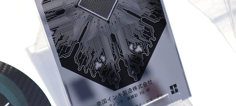
1. Ink for electromagnetic wave shield that contributes to cost reduction, lighter weight and thinner shape
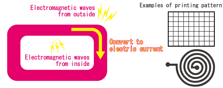
1. Structure of Ink for Electromagnetic Wave Shield
Electromagnetic wave shield ink is an ink that has both a conductive function and screen printing suitability. By printing this ink in an optimal circuit pattern on the housing, etc., according to the internal structure of the electronic equipment, it is possible to reduce leakage of internally generated electromagnetic waves and penetration of externally generated electromagnetic waves.
2. Comparison of Electromagnetic wave shield and other shield technologies
The comparison between ink for electromagnetic wave shield and other technologies is as follows. In particular, it is superior in cost reduction, thinner and lighter products
| Technology | Cost | Features |
|---|---|---|
|
Ink for electromagnetic shield |
Simple and inexpensive process |
|
|
Film for electromagnetic wave shield (Mesh type) |
More expensive than printing due to pasting process |
|
|
Metal foil, Forming metal thin film |
More expensive than printing |
|
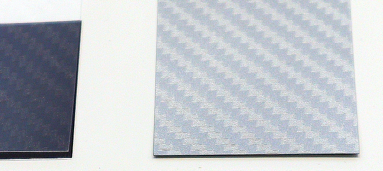
3. Application of Ink for Electromagnetic Shield to Display
Ink for electromagnetic wave shield can achieve both light transmittance and electromagnetic wave shielding function by devising printing patterns (see above). This makes it possible to replace mesh-type electromagnetic wave shielding films used in places where light transmission is required, such as displays. Replacing film with printing will help reduce manufacturing costs and make displays thinner and lighter.
Example of pattern printing of electromagnetic wave shield ink on a panel printed with smoke clear
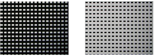
2. Introduction of Black matrix ink that contributes to significant cost reduction
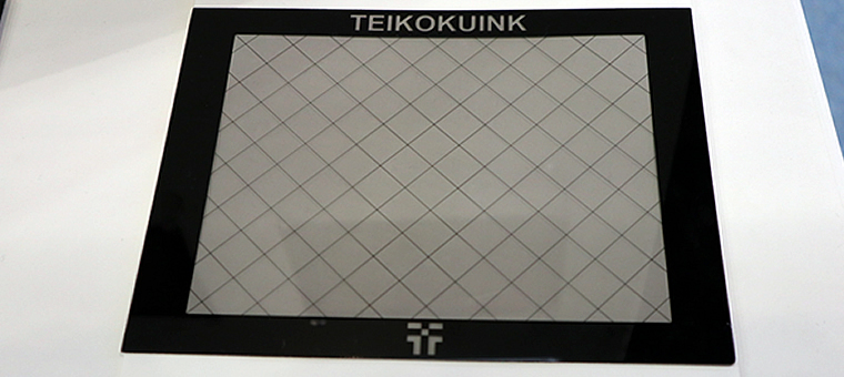
1. Black Matrix by screen printing
Black matrix ink is an ink that replaces the black matrix manufactured by photolithography with screen printing. Substitution is possible if the line width is 100 µm or more. (A smaller line width is also possible depending on the conditions. Please consult us.)
Example of Black Matrix printing (Narrow width: 100µm, Substrate: glass)
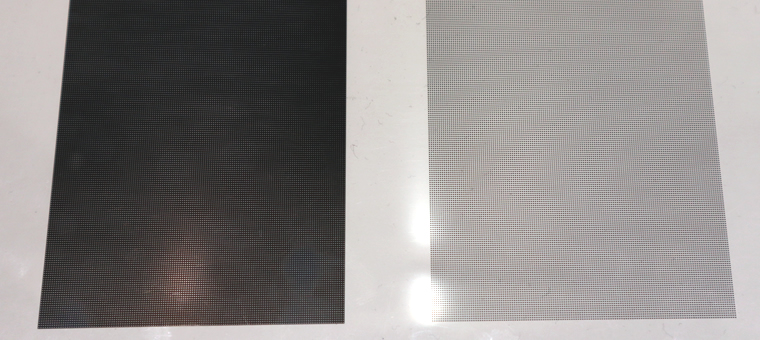
Enlarged photo of above black matrix
2. Comparison of Black matrix ink with other technologies
Comparison of Black matrix ink with other technologies is as follows. Black matrix inks are not as good as photolithography in terms of the line width that can be achieved, but they can greatly contribute to process simplification and cost reduction as long as substitution is possible.
| Technology | Cost | Features |
|---|---|---|
|
Black matrix ink |
Simple and inexpensive process |
・100µm (Please ask us for thinner line width) |
|
Photolithography |
Complex and expensive equipment and process |
・Fine lines of several µm level is possible, which is impossible with screen printing |
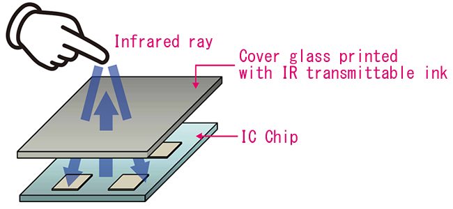
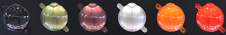
3. Introduction of Ink for sensor (IR transmittable ink) that realizes seamless design
1. Structure of Ink for sensor (IR transmittable ink)
Ink for sensor (IR transmittable ink) transmits only the light of the wavelength that the sensor wants to detect (infrared light in the case of a fingerprint authentication sensor) out of the light applied to the printed ink layer, blocks other light (visible light and ultraviolet light) that may cause malfunctions. With ink for sensor, it is possible to simultaneously improve the freedom of design using various colors and the accuracy of the sensing function.
Structure to use ink for sensor (IR transmittable ink) for fingerprint authentication sensor
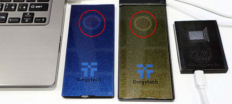
2. Seamless design by Ink for sensor
When sensor ink is applied to the fingerprint authentication sensor, the light-receiving part of the IR sensor that detects fingerprints can be decorated in the same way as the housing, allowing seamless design without interruption. It is also possible to add an IR transmission function to glittering pearl ink.
Example of seamless design with IR receiving part of fingerprint authentication sensor and housing (red circle)
4. Introducing a new design with movement by concealing printing
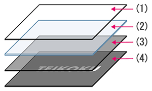
1. Concealing Printing that control transmission of visible light
Concealing printing is an ink that set to transmit light wavelengths in the visible light range. This is a printing method that express a design that was not imagined before the backlight was illuminated.
(1) Surface: Matt clear layer (2) PC substrate (3) Back: 1st layer: IR Transmittable Ink (4) Back: 2nd layer: Black outline printing
(1) Printing (2) Forming (3) Backlight irradiation (Characters appear!)
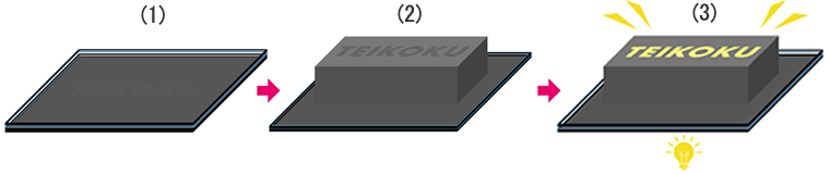
2. Example of applying concealing printing to design
Combination with concealable ink makes it possible to apply to unexpected designs, warning light and other decorations with message.
The impression changes greatly between normal (upper photo) and backlight irradiation (lower photo). (Left is high opacity black ink)
5. Realize high-grade image by highly accurate printing. Introducing High Definition Ink system (High Quality/High Definition screen ink)
1. 7 benefits of High Definition Ink system (High Quality/High Definition screen ink)
High-Definition Ink possess seven benefits, such as reduced printing processes and improved workability, as well as fine printability.
| Benefit | Features |
|---|---|
|
Benefit 1: Fine Printability |
L/S (line and space) 100µm fine line can be printed stably with a sagging width of 5 to 8µm on one side. ・30µmの細線・抜き印刷の実績もあり Proven track record of 30µm fine line and outline printing |
|
Benefit 2 : Simultaneous printing of solid and fine lines |
Mixed design of solid print, gradation and fine line can be printed on one stencil. |
|
Benefit 3 : Countermeasure for saw edge |
Realize perfect straight line and circle with a saw edge 10µm or less(unevenness at printing border). |
|
Benefit 4 : Continuous printability |
Continuous printing of 1500 sheets without changing of fine lines and dots |
|
Benefit 5 : High-speed printability |
Fine printing is possible with a cylinder printing machine at 800 to 1500 sheets / hour. |
|
Benefit 6 : Re-printability |
Printing can be resumed even after the press has been stopped for one hour |
|
Benefit 7 : Reduction of number of cleaning stencil |
Stencil cleaning reduced from once every 300 sheets to once every 1500 sheets |
2. Provide high grade image by fine printability
Fine printability of this High Definition Ink enables luxurious feeling design that has not ever been realized.
A luxurious modern design combining High Definition Ink and mirror ink (base material: glass, line width 100µm)
3. New expression by application of fine printability
The fine printability of High Definition Ink can express a new texture never seen before by applying it to three-dimensional printing.
Example of 3D design by High Definition Ink
6. Introducing decorative technology to curved glass
Application to curved display glass
Glass display for smartphone have come to use curved surfaces to improve portability and design. In conventional screen printing technology, printing on curved surfaces had been difficult, but it has become possible to apply pad printing and print on curved surfaces using a screen printer that supports curved surfaces.
Example of glass window frame printing using a curved surface for the window frame
Example of wide color variation
7. Functional Black Ink(1): Introducing Piano Black Ink
1. Comparison with ordinary black ink by color measurement value (SCE, Specular Component Exclude Method)
Piano Black Ink (Jet Black Ink) expresses deeper black color than ordinary black ink. Even with the SCE (Specular Component Exclude) method measurement, jet blackness with a brightness L value of 0.70 with 1.0 or less is realized.
| SCE | Ordinary Black Ink | Piano Black Ink | |
|---|---|---|---|
|
Color difference |
L* |
4.97 |
0.70 |
|
a* |
– 0.15 |
0.27 |
|
|
b* |
0.80 |
1.03 |
|
2. Piano black ink that produces a sense of high grade quality
Piano black ink expresses deep black that ordinary black ink cannot express. This deep black color contributes to the elegance and luxury of the product like a lacquered luxury product.
Black depth of piano black ink (left) clarified by light irradiation (right is normal black ink)
Functional Ink Black (2): Introduction of ink for glass (GIZ-HF) with excellent post processing
1. Excellent post processing due to high resistance to Glue (resistance to adhesive agent, double sided tape)
GIZ-HF is a screen ink for glass that possess high glue resistance (resistance to adhesive agent, double sided tape). This high glue resistance contributes to the improvement of quality of post processing such as bonding process using decorated glass adhesive agent.
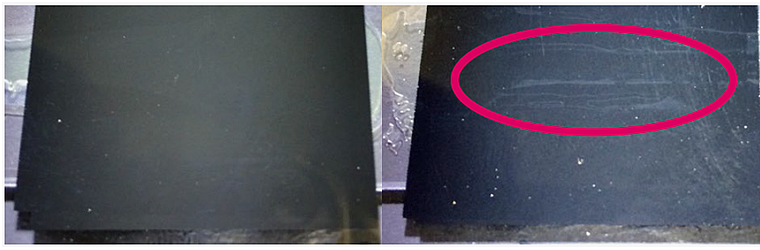
Printed ink layer of GIZ-HF that is not affected by component of adhesive agent and double sided tape (left) and printed ink layer of ordinary ink that is affected by (right).
2. High Dyne value prevents cissing on printed ink layer
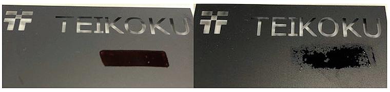
GIZ-HF 939 NC Black raised dyne value related to surface tension from about 35 to more than 42. This high dyne value solves the problem of cissing at the overcoating process after printing.
Printed ink layer of GIZ-HF939 NC BLACK that does not repel marks painted with a pen (left) and normal printed ink layer that repels (right)
8. Introduction of clear for display contributes to improvement of visibility
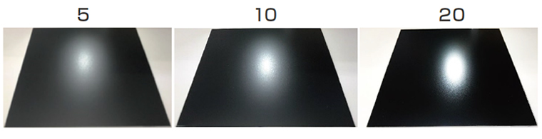
Clear with freely adjustable optical properties (glossiness・transmittance)
Clear for display can freely adjust the gloss value, which is the glossiness that reflects external light, and the haze value, which is the light transmittance. The ability to set freely these optical characteristics enables anti-glare (anti-reflection) and transparency settings according to the display usage environment, and greatly contributes to improvement of visibility.
Example of printing clear on display (From left, Gloss value 5, 10, 20.)
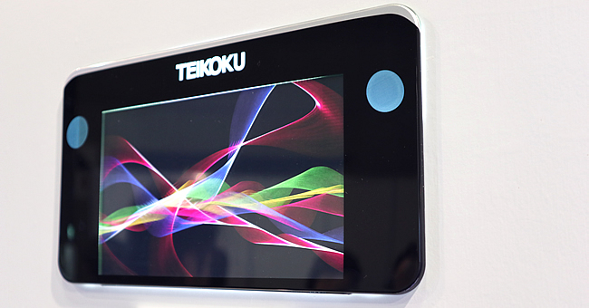
9. Contributes to light weight and cost reduction of Display. Introduction of FIM (Film Insert Molding)
1. FIM (Film Insert Molding)
FIM (Film Insert Molding) is a method of creating a product by integrating a pre-designed thermoplastic resin film with a molding resin material.
(1) Screen Printing (2) Forming (3) Injection
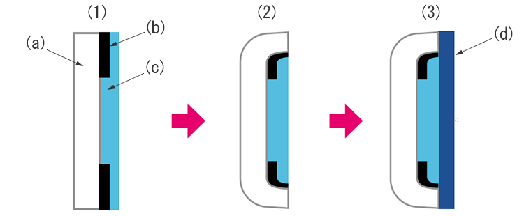
(a) Resin sheet (b) Ink layer (c) Binder layer (d) Molding resin
2. Realization of weight reduction and cost reduction by replacing glass
By using FIM technology, it is possible to convert display panels from glass to resin and reduce the weight. Also, since the decoration process of FIM is simpler than the glass decoration and assembly process, significant cost reductions can be expected.
Display integrated with housing using FIM technology (realizes rounded corners)
- Related technical information
-
- Electromagnetic wave shielding ink
- Introduction of 7 benefits
- Introduction of High Quality and High Definition Screen Printing Ink
- Ink for sensor
- Introduction of GLS-HF ink(1)
- Introduction of High-Definition Ink (high-quality, high-definition screen ink)
- Introduction of GLS-HF ink(2)
- Introduction of functional Black ink
- Introduction of High-Opaque Black and High-Opaque White
- Introduction of Non-Conductive Black ink
- GIZ-HF ink series excellent resistance for solvent and adhesive
- Introduction of MIX-HF ink(3)
- High Definition Ink System for Molding
- Introduction of new decoration of PP resin products.
- Technology lecture for FIM/IMD 1st session: Explanation of the merit and 3 process.
- Related event information
Please feel free to contact us about the inks, methods, and trial products we have introduced.